


 Copy to clipboard
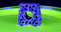
The future of orthopaedic medical devices is small—microscopically small. Microelectromechanical Systems, referred to as MEMS devices or sensors, are already used in a host of medical devices, doing tasks that were previously only conceived of in science fiction.
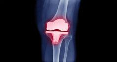
Sensors the size of a flea can now measure strain, temperature or resistivity. They can measure acceleration, frequency and electrical impulses. MEMS can be used to make microscopic gears to tune hearing aids, capacitive rings embedded in contact lenses to measure glucose levels and microfluidic pumps to deliver insulin to patients. Little of this technology has infiltrated the orthopaedic device market, which tends to be conservative and use established, trusted techniques. Recently, however, some companies have successfully incorporated sensors in devices like total knee arthroplasty balancing instruments that measure the applied load to optimize the selection of the polyethylene tibial component’s thickness.
Adding functionality and capability makes sense in orthopaedics, because we all want to provide our customers with more feedback and diagnostic information and we definitely want to continuously improve patient outcomes. Thus, it will be a short time before new products are introduced with embedded electronics and sensors. To capitalize on this paradigm shift, now is the time to learn how to incorporate MEMS into your next big design idea.
Getting Started
This article will cover what MEMS is, how a device or sensor is fabricated and where public laboratories are located. In a second article, I’ll cover ways to collaborate with a public laboratory and will include the main types of equipment in these facilities. I’ll also discuss intellectual property and privacy issues, as well as ways to navigate other issues that may arise.
Ideas for where and how MEMS could be used in your orthopaedic device are limited only by your imagination. I can envision instruments and implants that provide feedback to the surgeon or the patient, devices that measure the strength of bone or sense the location of an artery, nerve or cameras that guide the placement of screws. The key is to understand MEMS technology and its possibilities so that you know how to use it in your design.
What is MEMS?
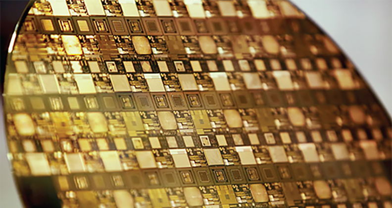
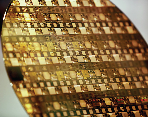
MEMS is an etching-based machining technique done on silicon wafers. Sometimes, layers of material are first deposited, but etching away material is usually required. This allows easy fabrication of features with micron-level dimensions. Do you need a strain gauge that is only a fraction of a millimeter in size? MEMS is the answer; in fact, these are called semiconductor or piezoresistive strain gauges, and you can buy them off the shelf. They are adhesively mounted and attached with wire leads the same way as copper foil strain gauges, except that a microscope and a steady hand are required. In spite of being tiny, they are actually 100 times more sensitive than copper foil strain gauges, because they respond to changes in the crystalline structure. The disadvantage is that they produce a nonlinear response, so they have to be used with a correlation curve or equation to interpret.
As an example, to create a MEMS strain gauge, you need to think in terms of patterned layers. Your silicon wafer, usually 100 to 200 mm (4 to 8 inches) in diameter and 600 µm (0.024 inches) thick, can be polished on one or both sides. Let’s assume that you want to use a single-sided wafer for this device, as you plan to make your strain gauge the full thickness of the wafer.
How do you fabricate a MEMS device?
First, you work at your computer with a specialized CAD program to create layers to pattern your wafer. These layers represent each of the processing steps required to fully fabricate your device, such as the size and shape of the looped “wire” of your strain gauge, the soldering tabs and the mote with tethers around each strain gauge to allow you to easily break them free from the substrate.
Next, you fill your wafer with as many copies of the strain gauge as you can fit. This can be anywhere from 100 to a 1,000, depending on how densely you can package them and the diameter of the wafer you’re using. Then, you either make or send out your patterns to make masks for each layer. The mask can either be a positive or a negative mask, depending on whether or not you want to expose the feature to be etched or expose the negative space around the feature to be etched.
At this point, you need to gown up and enter the cleanroom. There are multiple MEMS labs that are available for public use. (We’ll go into how to find these facilities and train to use them later in this article.) Let’s assume for now that you identified a lab and are trained. Your first stop in the lab will be to passivate your wafer to remove free electrons. Then, you’ll clean and spin dry your wafer to remove dust or ash that may have accumulated on the surface. It is impossible to tell if your wafer is contaminated, so you’ll assume that it is.At this point, you need to gown up and enter the cleanroom. There are multiple MEMS labs that are available for public use. (We’ll go into how to find these facilities and train to use them later in this article.) Let’s assume for now that you identified a lab and are trained. Your first stop in the lab will be to passivate your wafer to remove free electrons. Then, you’ll clean and spin dry your wafer to remove dust or ash that may have accumulated on the surface. It is impossible to tell if your wafer is contaminated, so you’ll assume that it is.
Silicon wafers can be wet or dry etched to design a pattern. Wet etching uses a chemical bath to eat away at the exposed portions of the wafer. Dry etching involves introducing ions on the surface of the wafer. Various methods can be used and the processes can take several hours to multiple days.
Wafers are usually patterned with high intensity light. This is called photolithography. You first spin coat on a micro-thin layer of a photosensitive film, then place your mask for the first layer into a specialized machine between the light source and your coated wafer. A few seconds of light exposure, and the parts of the film that were exposed by the mask are degraded in a way that allows the material to be washed away in a chemical bath, revealing the silicon wafer again.
As with the microscopic contaminant, you often cannot see the pattern that you’ve created on the wafer with your naked eye. You would have to look at it under a microscope, but this isn’t advised, as this can potentially expose your pattern to harmful light, even if you use a special filter. So, you again assume that all is well and proceed to etching or build-up. Let’s use an etching and material removal process for our strain gauge example.
Etching can be either wet or dry. Wet etching uses a chemical bath to eat away at the silicon wafer wherever it’s exposed. The shape and depth of the etch depend on several factors, including obvious ones like time and the chemical used, and not-so-obvious ones like the crystal orientation in your chosen wafer. If the wafer has Miller index orientation of <100>, that means the face of the crystal lattice is normal to the face of the wafer. The other axis is determined by a flat on the circumference of the wafer. During etching, the chemicals eat away along some crystal planes more rapidly than others, so if your goal is to produce a trapezoidal feature, you’ll choose one orientation, perhaps a <111>. If you want more rectilinear walls, you’ll choose a different one. Not to overly complicate the choices available to you, but you can also choose what type of doping you want, whether there are an excess or lack of electrons available. All of these choices, however, are not something you need to determine by yourself. All facilities have staff that can help you choose the most appropriate wafer for your project.
Dry etching involves bombarding the surface with ions. The area protected by the film is not etched. This is called reactive ion etching (RIE) or deep reactive ion etching (DRIE). The advantages of dry etching are numerous. First, it’s much easier to get straight walls on your features. Second, you can etch much deeper (on the order of 40 µm) and maintain very tight tolerances of 1-2 µm. Third, there are fewer variables to consider. Even though the setup is more complex, it’s easier to control the outcome and maintain consistency between setups.
Other steps may involve adding material, such as metal for our soldering tabs. This is called vapor deposition. Although the material is deposited uniformly across the wafer, that which is on top of the film is washed away, leaving metal adhered only where desired.
You repeat the steps of: spin coat on a film, pattern, etch or deposit and rinse for as many mask layers as you have in your design. This can be as few as three or four or as many as 40 or more. Along the way, you may choose to microscopically evaluate or measure a feature to ensure that it meets your requirements. Some processes can take several hours, others just minutes—it’s not uncommon for a single wafer to take multiple days to complete. Eventually, once you’re done, you take your wafer out of the cleanroom and either break or dice your devices out of the wafer. They may be simple mechanical devices like our strain gauge, or they may be sensors integrated with circuitry or surface mount solder features to incorporate into a printed circuit board.
Where are facilities that are available for public use?
The National Nanotechnology Coordinated Infrastructure (NNCI) is a network of 16 institutions across the U.S. Most are affiliated with one or more universities. For instance, the one I’ve used is at the University of Washington, but Oregon State University is a partner institute and has additional equipment and resources available. The map below shows site locations. Equipment available at these facilities varies widely. It is best to review the website for more detailed information. You can find a list of more than 2,000 pieces of equipment, a list of experts at each facility and more.

Interestingly, several of the labs are conveniently located near existing orthopaedic manufacturing hubs, such as Austin, Boston, Minneapolis, Philadelphia, Portland and San Diego, making them accessible to your current workforce.
How to Work with an NNCI Facility
The first step is often a discussion with the facility’s director. Each facility’s principal investigator and their contact information are listed on the organization’s website, along with a NSF Award Abstract, which gives a summary of each facility’s mission, capabilities and additional networking information.
For me, this initial discussion included nondisclosure agreements, and we met in a conference room at the University of Washington, where we had a design review of my project. Experts from the facility weighed in with their ideas and we developed a training plan for my use of the lab. Over the next several weeks, I filled out a user agreement, arranged short-term, summer housing at the university, researched a convenient means of commuting on public transit and proceeded to work my way through the training I needed. This began with safety protocols then stepped through gowning procedures for the cleanroom, use of microscopes and how to clean and spin coat a film on a wafer. Rather than overwhelm me with too much information at once, the lab staff demonstrated each piece of equipment I would need one at a time, allowing me to practice and then use that equipment before reading the training materials for the next step.
It took about two months to complete the training I needed, at which point I was then free to use the equipment. I spent about two years working at this facility, a few days per week during the summer and once or twice per month during the academic year. I fabricated two complete design iterations of my device.
Your use of a facility will depend on your needs. It is not necessary to go into the cleanroom yourself and do the fabrication. Each facility has expert staff that can do the design research and fabrication for you. In addition, most of these facilities are housed at a university and you can sponsor a student research assistant to pursue your design. Finally, some facilities, like the University of Washington, rent desk space to employees from private companies at their lab. These employees work for industry and conduct full-time research in the lab. So, there are numerous avenues available to you to pursue inclusion of MEMS in your next design idea.
Tiny Times are Upon Us
This is an exciting time in orthopaedics, as new technologies regularly become accessible for us to use in our products. MEMS is one tool that can bring increased functionality and capability to our designs, thus providing more diagnostic information and hopefully improving patient outcomes.
Collaborating with a public lab will create questions and new challenges, such as with intellectual property and ways to interface effectively with employees at a separate work location. These topics and more will be covered in a second article about how to incorporate MEMS into your next design project.
Dr. Deborah Munro is the President of Munro Medical, a biomedical research and consulting firm in Portland, Oregon. She has worked in the orthopaedic medical device field for almost 20 years and holds numerous patents, mostly in the area of spinal fusion. She taught mechanical and biomedical engineering at the University of Portland for eight years, where she also founded a Master’s in Biomedical Engineering program. Her current interests include developing new medical device solutions for companies and assisting them in their regulatory compliance efforts. She can be reached by email.